3D-Integration

Technology offers for 3D-Integration

The integration of heterogeneous components using 3D technologies is crucial for future system scaling, especially in high-performance, low-power systems where computing and memory functions are optimized and integrated.

Within the PREVAIL framework, the RTOs (IMEC, CEA-LETI, FhG) are developing new 3D technology flows for edge AI applications, leveraging their existing and expanded technological capabilities to propose new combined 3D offerings, such as Si Interposers with front- and backside RDL, mixed pitch interconnect formation, Die-to-Wafer assembly, TSV formation and/or singulation.

The three RTOs offer a broad portfolio of 3D 300 mm Si wafer technologies, enabling the integration of dedicated building blocks into edge AI systems, which significantly enhance system performance and integration density. Additionally, VTT provides building blocks for smaller wafer sizes (200 mm and below) to support 3D integration on those sizes.

Services linked to fabrication will be available during the TEF operation, with details announced during Q4/2024-Q1/2025.

Through-Silicon Via (TSV)

Through-Silicon Via (TSV) technology addresses the limitations of traditional two-dimensional integrated circuits (2D ICs) by creating vertical electrical connections between the front and back sides of silicon wafers or dies. This allows for the interconnection of multiple chips, memory, sensors, and other modules, resulting in smaller, faster, and more power-efficient devices.

Key Advantages of TSVs:

  • Reduced Signal Propagation Delay: Data signals travel vertically through the thinner silicon substrate, significantly reducing signal propagation delay.

  • Lower Power Consumption and Area: Shorter interconnect lengths reduce the overall area and power consumption of the chip, making TSVs ideal for high-speed applications such as data centers, servers, GPUs, AI-based processors, and wireless communication devices.

    • Heterogeneous Integration: TSVs enable the combination of multiple chips from different technologies and manufacturers, facilitating heterogeneous integration.

    The PREVAIL TEF will offer TSV solutions that are fully integrated with CMOS technologies, enhancing the performance and efficiency of various high- speed applications.

    The choice of TSV technology depends on the final application, but usually a combination of technologies is used. Our offer will start with:
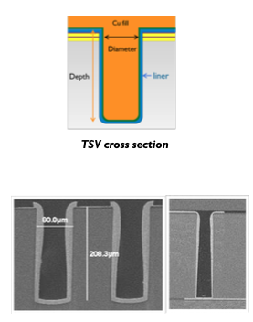
    Via Middle

    In this type of technology, TSVs are created after the active circuitry is fabricated on the wafer but before the fabrication of metallization layers (BEOL, i.e., the back end of the line). This Via Middle approach is primarily used to connect both the active and passive layers of the integrated circuits through TSVs. This approach is mainly used in applications such as microprocessors and memory devices.

    Via Last

    In this type of technology, TSVs are fabricated after the fabrication of active layers, i.e., FEOL, and after (or during) the metallization layers, i.e., BEOL. This Via Last approach connects the TSVs to the external package or substrate through a metal redistribution layer (RDL) and an interconnections like Cu pillars or solder bumps. This approach is often used in microelectronic systems.

TSVs last with aspect ratios of 2 and 5, respectively

Advanced 2.5D, 3D and heterogeneous die stacking technologies require increasingly denser interconnects with reduced die separation, improved thermal performance, and high current carrying capabilities.

Within PREVAIL TEF, different types of fine pitch interconnects will be offered:

• Die-to-Wafer Bonding Using Microbumps

The state-of-the-art microbump pitches in production have saturated at about 30μm. Using material innovations, interconnect pitches down to 7μm could be demonstrated. Such high-density connections leverage the full potential of Through- Silicon Via technology, enabling more than 16 times higher 3D interconnect densities.

Figures courtesy of imec

• Die-to-Wafer Bonding Using Hybrid Bonding Solutions

Hybrid bonding solutions with pitches down to 3μm are possible in this case. Hybrid bonding allows for very high interconnection densities, ranging from (10^4) to (10^6) interconnections per mm2. The die-to-wafer approach is more flexible and cost-effective compared to the classical wafer-to-wafer approach. This method allows the use of Known Good Dies (KGD) to improve the final yield of the assembly and enables the integration of chips from different sources. Another advantage is the ability to reduce the inter-die spacing to a few microns for the chip matrix assembly.

P. Metzger et al., Minapad forum 2022

For more information, sign up to be part of or PREVAIL network and receive first-hand news of the project. For detailed technical enquiries regarding our offer and access, please fill in the PREVAIL enquiry form.

Disclaimer: The information on this website is for general purposes only and may be modified without prior notice. For detailed information about our offers and services, please contact the PREVAIL User Interface Team directly via the Enquiry Form.