
In recent years, state-of-the-art Photonics Integrated Circuits (PICs) have enabled ultrafast artificial neural networks, offering an enhancement in computational speed and power efficiency. Algorithms running on such hardware have the potential to address the growing demand for machine learning and artificial intelligence in areas such as medical diagnosis, telecommunications, and high- performance and scientific computing. In PREVAIL, the consortium partners, IMEC and CEA Leti hold a world-leading position in this field, proposing cutting-edge PIC processes.
Services linked to fabrication will be available during the TEF operation, with details announced during Q4/2024-Q1/2025.
IMEC’s iSiPP300 platform
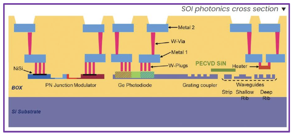
IMEC’s iSiPP300 platform integrates a variety of passive and active components on SOI substrates using advanced 193 nm-immersion lithography, enabling sub-100 nm patterning and deep sub-wavelength structures. The key building blocks of IMEC Silicon Photonics technology offered in the PREVAIL pilot line is the PECVD SiN edge coupler module and silicon undercut module (UCUT). IMEC also supports chip stacking with Through Silicon Vias and micro-bumps, crucial for electrical-optical interfaces in data transmission and computing.
Key technology parameters:
Starting substrate: Silicon-on-insulator with 220nm Si / 2000nm BOX
3-level Si & 1-level poly-Si patterning with 193nm lithography
6-level silicon doping & 2-level Ge doping
Ge-on-Si RPCVD epitaxy
2-level Cu interconnects + Al bond pad
Deep-Si etch for edge coupling
Building blocks available:
Si, PEC VD SiN edge couplers
Encapsulated local substrate undercut
Embedded TSV’s in the silicon photonics platform which can enable PIC face-up assembly flows
Available devices:
Silicon Ring Modulator
GeSi Electro- Absorption Modulator
Silicon Mach-Zehnder Modulator
Ge Photodetector
SMF Grating Coupler (<2dB)
SMF Edge Couplers (<3dB)
Efficient Thermo-Optic Phase Tuners
High-density Si Waveguides (0. 5-2dB/cm)
Silicon WDM filters
Baseline cross-section of imec’s Silicon Photonics 300mm platform available via PREVAIL, indicating some basic devices
IMEC’s complete PDK encompasses IMEC’s Silicon Photonics iSIPP300 technology handbook, design rules, and models necessary for the design and layout of Photonics integrated circuits and library components.
Module | Content | EDA Tool Compatibility |
|---|---|---|
CAD layer list | CSV-file | NA |
CAD layer display settings | LYP-file | KLayout |
Standard waveguide cross-section definition | YAML-file | NA |
Device library | GDSII files; XML component- interface description; CSV files with component specs | NA |
DRC | Encrypted deck file | SIEMENS EDA – Calibre |
Doc | Design rule manual, including device library component information | NA |
Summary of IMEC’s Silicon Photonics PDK
CEA-Leti’s photonics platform
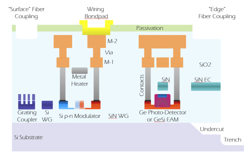
CEA-Leti’s photonics platform also co-integrates a wide variety of passive and active components that were initially designed for short-reach optical interconnects and have progressively been expanded to applications in sensing and artificial intelligence. The technology is based on SOI substrates with a silicon thickness of 310nm and BOX thickness of either 720nm or 2000nm. 193nm-immersion lithography is used, enabling sub-100nm patterning. The competitive advantage of this technology over deep UV lithography has been demonstrated with, for instance, low-loss optical chip-to-fiber couplers, low-loss waveguides, and enhanced repeatability of the devices’ performance. Different high speed modulator options are available (PN and PIN junctions) as well as photodetectors (PD). Nine different doping levels are possible to optimize the junctions for analoge bandwidth and efficiency. In addition to the 310nm height Si waveguide layer, a PECVD SiN waveguide layer is provided with a 600nm height. Thus, the optical coupling can be realized with efficient surface grating couplers or edge couplers. In the back end of line, one heater layer, two Cu metal levels, and an aluminum pad layer are provided for electrical interconnects (wirebonding or flip-chipping).
For PREVAIL, the Silicon Photonics platform cross-section is given below, illustrating the different layers accessible to the users. Not represented are the aluminum bond pads layer as well as the edge couplers (deep trench to substrate).
Key technology parameters:
Starting substrate: Silicon-on-insulator with 310nm Si / 720nm or 2000nm BOX
3-level Si patterning with 193nm lithography
9-level silicon doping
Ge-on-Si epitaxy
2-level Cu interconnects + Al bond pad
Deep-Si etch for edge coupling
Available devices:
High speed PN modulation junction ( VpiLpi<1. 5 V. cm with B W>30GHz)
Si-Ge-Si Photodetector (~1A/W, BW > 45GHz)
SMF Grating Coupler (<2dB)
SMF Edge Couplers (<3dB)
Efficient Thermo-Optic Phase Tuners (<6mW/pi with insulating trenches)
High-density Si Waveguides (0. 35-1. 1dB/cm in C-band, 0. 4-1. 2dB in O-band)
Silicon WDM filters in both Si and SiN layers
Schematic description CEA-Let’s photonics platform with PECVD SiN
CEA-Leti’s complete PDK comprises the Silicon Photonics technology handbook and design rules manual, enabling the design and layout of photonic integrated circuits and library components.
Module | Content | EDA Tool Compatibility |
|---|---|---|
CAD layer list | CSV-file | NA |
CAD layer display settings | LYP-file | KLayout |
Standard waveguide cross-section definition | YAML-file | NA |
Device library | GDSII files; XML component- interface description; CSV files with component specs | NA |
DRC | Encrypted deck file | SIEMENS EDA – Calibre |
Doc | Design rule manual, including device library component information | NA |
Summary of CEA-Leti’s Silicon Photonics PDK contents
For more information, sign up to be part of or PREVAIL network and receive first-hand news of the project. For detailed technical enquiries regarding our offer and access, please fill in the PREVAIL enquiry form.
Disclaimer: The information on this website is for general purposes only and may be modified without prior notice. For detailed information about our offers and services, please contact the PREVAIL User Interface Team directly via the Enquiry Form.
PREVAIL project partners
PREVAIL
A multi-hub Test and Experimentation Facility for edge AI hardware

Grant Agreement No. 101083307