
Embedded non-volatile memories (eNVM), designed to retain data even when power is off, have become an important and essential IP. High retention eNVM technologies are well-suited for applications where data retention is crucial, such as firmware in microcontrollers, IoT devices, and other embedded systems at 28nm and below nodes, where standard embedded flash becomes prohibitively expensive.
In addition to embedded-flash replacement applications, there is significant potential for high-performance eNVM to be used as cache replacement, replacing some of the SRAM chips. This enables higher bit density (compared to SRAM) and reduces standby power thanks to the NVM properties.
In PREVAIL, the RTOs (IMEC, CEA-LETI, and FhG) are gradually deploying three macro IPs mainly embedded in back-end of line of standard foundry CMOS process platforms, targeting edge AI. Our portfolio provides users with access to advanced technologies for Magnetoresistive Random Access Memory (MRAM), Oxide-based RAM (OxRAM), and Ferroelectric RAM (FeRAM). To fulfill customers’ need for continuous performance improvement and power-consumption reduction for edge AI applications, Prevail consortium is focusing on two types of offerings:
Access to off-the-shelf test vehicles: The RTOs provide a broad portfolio of test vehicles manufactured in a CMOS back-end-of-line process, allowing customers to validate the performance of their stacks and extract useful information that will lead to further optimization of their technology. This enables customers to perform reliability and performance characterization of dedicated array test structures that mimic the real operations of a fully functional integrated product and provide sufficient bit count for statistical analysis.
Access to fully CMOS logic compatible PDKs for user custom device design: The consortium will be providing Process Design Kit (PDK) add-ons, enabling the design of circuits in these technologies and specific to each integration flow. PDKs will contain the description of NVM-specific layers and, when available, PCells to enable and facilitate the layout. For electrical simulations, they will include specific analog design libraries, solid compact models calibrated on hardware data, and parasitic descriptions. With these tools, users will be able to autonomously design IP blocks according to their own specifications.
Services linked to fabrication will be available during the TEF operation, with details announced during Q4/2024-Q1/2025.
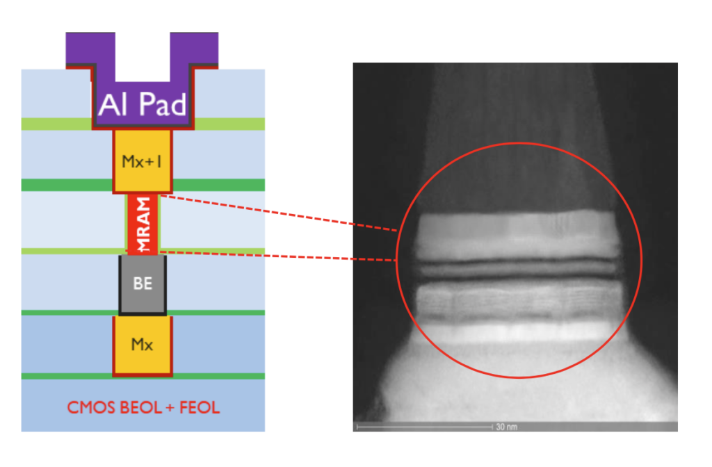
IMEC is establishing a BEOL flow that allows the incorporation of STT-MRAM technology on top of foundry CMOS front-end wafers currently at the 22nm node. The technology includes a bottom electrode module that enables an ultra-smooth, TaN-based bottom layer onto which the MRAM stack is deposited. The top electrode module then enables a dual damascene Cu-based wiring to land on the top of the MRAM pillar, after which standard back-end-of-line processing can resume.
NVM technology | STT-MRAM Spin-Transfer Torque – Magnetic Random Access Memory |
|---|---|
Technology characteristics Special features
(Main benefits / uniqueness) | Non-volatile memory (no leakage) with read/write speed of 10ns or below |
Application area (Targeted applications) | • AI: compute in memory • Low standby power high performance MCU for IoT applications |
Pitch/Cell Dimension nm/nm | 208/50 |
Integration | Between M6 and M7 |
PDK | V.1.0.0 (In preparation) |
Frontend/backend | Cadence – Virtuoso |
Verification tools | DRC Calibre |
Library | The PDK includes process documentation, library devices, layout guidelines for custom design, verification and models. |
Process option | 22 nm FD-SOI |
STT-MRAM process flow
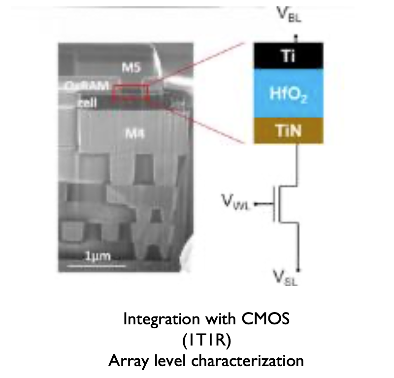
CEA will deploy a Hafnium Oxide-based resistive-switching random access memory currently implemented as a 1T1R structure, i.e. with one MOS transistor (1T) used for accessing one resistor (1R). The memory cell footprint is around 40F2 and is limited by the access transistor, already in 28nm FDSOI technology but soon in 22nm. To achieve high density, it is also possible to increase the number of resistance levels in a single cell, for storing multiple bits.
NVM technology | OxRAM Oxide-based – Random Access Memory |
|---|---|
Technology characteristics Special features
(Main benefits / uniqueness) | • Low cost embedded Non-Volatile Memory (few added mask to CMOS planar technology) • Low power solution |
Application area (Targeted applications) | • Storage: eFlash replacement • AI: compute in memory |
Pitch/Cell Dimension nm/nm | • Pitch 360nm / device size 170 nm |
Integration | • In the BEOL (1st metal above the existing IPs, so could be between M4-M5) |
PDK | PDK addon, v1.0 available |
Frontend/backend | • Cadence – Virtuoso (design) & Spectre (Simulation) |
Verification tools | • Electrical verif (SPICE) Cadence – Spectre, physical (DRC/LVS) Siemens – Calibre |
Library | The PDK includes process documentation, library devices, layout guidelines for custom design, verification and models. |
Process option | 22 nm FD-SOI |
Resistive Random-Access Memories or Memristors (RR AM)

FHG is working on a ferroelectric field effect transistor (FeFET) technology, based on hafnium oxide layers integrated in the gate of standard MOS transistors. The bitcell size is therefore mainly defined by the sizing of the transistors and additional programming circuitry. As the ferroelectric layer is integrated in the gate/poly structure of 28nm technology, the integration of such devices happens in the front-end of line process flow, requiring close collaboration with the foundries. In this case, the technology will be embedded in the 28nm technology by adapting transistors to the size needed for robust programming and sufficient memory window.
NVM technology | FeFET Ferroelectric Field Effect Transistor – based NVM |
|---|---|
Technology characteristics Special features
(Main benefits / uniqueness) | • eFlash replacement w/o charge pump:
i.e. smaller footprint combined w/ low additional costs and increased energy efficiency |
Application area (Targeted applications) | • e-flash replacement in planar node • SRAM replacement in planar node • High density crossbar array |
Gate width/Gate length | 450/450 or 180/180 nm |
Integration | FEoL |
PDK | V.1.1 |
Frontend/backend | Cadence – Virtuoso |
Verification tools | DRC Calibre |
Library | The PDK includes process documentation, library devices, layout guidelines for custom design, verification and models |
Process option | 28 nm FD-SOI BEoL metal stack |
Ferroelectric field effect transistor (FeFET)
For more information, sign up to be part of or PREVAIL network and receive first-hand news of the project. For detailed technical enquiries regarding our offer and access, please fill in the PREVAIL enquiry form.
Disclaimer: The information on this website is for general purposes only and may be modified without prior notice. For detailed information about our offers and services, please contact the PREVAIL User Interface Team directly via the Enquiry Form.
PREVAIL project partners
PREVAIL
A multi-hub Test and Experimentation Facility for edge AI hardware

Grant Agreement No. 101083307